



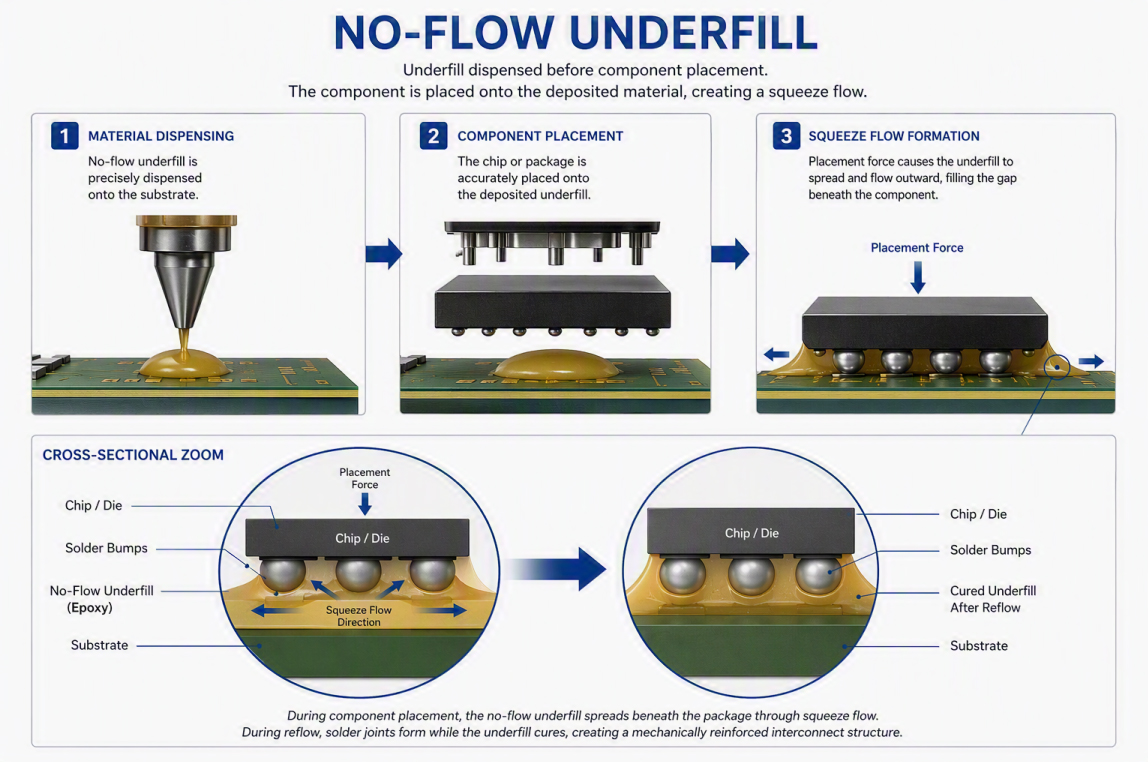
As semiconductor devices become smaller, thinner, and more complex, manufacturers need packaging solutions that support both high volume production and long-term reliability. No flow underfill is a specialized epoxy material designed to simplify semiconductor assembly by combining chip attachment and underfill formation into a single process.
Unlike traditional capillary underfill, which is dispensed after component placement and solder reflow, no flow underfill is applied to the substrate before the die or package is placed. As the component is positioned, the material spreads beneath the device through a controlled squeeze-flow action. During reflow, solder joints are formed while the underfill cures simultaneously, creating a reinforced package structure in a single manufacturing step.
This integrated process reduces manufacturing cycle time, increases throughput, and enhances package reliability, making it an attractive solution for advanced semiconductor packaging applications.
The no flow underfill process consists of three key stages:
No flow underfill is commonly used in:
Successful no flow underfill processes depend on accurate and repeatable material placement. Precise dispensing promotes consistent squeeze-flow behavior, complete coverage beneath the component, and reliable package performance. The ability to dispense customized or complex patterns helps optimize material distribution, reduce mechanical stress, and improve manufacturing yield.
Advanced automated dispensing systems provide:
GPD Global dispensing systems deliver the accuracy, repeatability, and process control required for modern no flow underfill applications. Designed for semiconductor packaging and advanced electronics manufacturing, our solutions help improve reliability, increase throughput, and ensure consistent material placement across every assembly.
Contact GPD Global to learn more about automated dispensing solutions for no flow underfill applications.
Read more about what is underfill
