



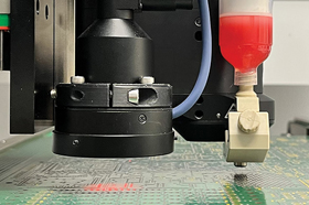
Solder paste jetting is emerging as a key solution for the precision demands of next-generation AI and data center hardware manufacturing. As a non-contact deposition method, it stands in contrast to traditional stencil printing, offering the flexibility needed as AI/HPC board architectures grow more complex.
Six core benefits stand out: no need for custom stencils, precise volumetric control for consistent solder deposits, better access to complex or crowded board areas, and support for mixed-component designs without sacrificing volume accuracy. These advantages translate directly into real-world applications, including AI servers, networking hardware, power electronics, high-density assemblies, advanced semiconductor packaging, System-in-Package (SiP) builds, and prototyping.
Ultimately, solder paste jetting is positioned as core infrastructure for scaling AI hardware production, giving manufacturers tighter process control and faster product development cycles.
Read the full article about Precision Solder Paste Jetting in Advanced Electronics Manufacturing
Please fill in the form to contact us about Dispensing articles.
