Solder Paste Jetting for Advanced Electronics Manufacturing
Solder Paste Jetting for Advanced Electronics Manufacturing
Precision Solder Deposition for Next-Generation AI Infrastructure
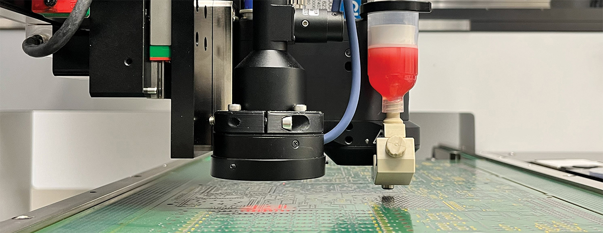
As artificial intelligence, cloud computing, and high-performance computing continue to push the limits of semiconductor and electronics design, manufacturers require more flexible and precise assembly processes. Solder paste jetting technology helps address these challenges by enabling accurate, non-contact solder deposition for complex electronic assemblies used throughout AI and data center hardware.
Unlike traditional stencil printing methods, solder paste jetting deposits precise volumes of solder paste exactly where needed without physical contact with the substrate. This provides greater flexibility when assembling densely populated circuit boards, advanced semiconductor packages, and high-performance computing systems.
Why Solder Paste Jetting Matters for AI Hardware
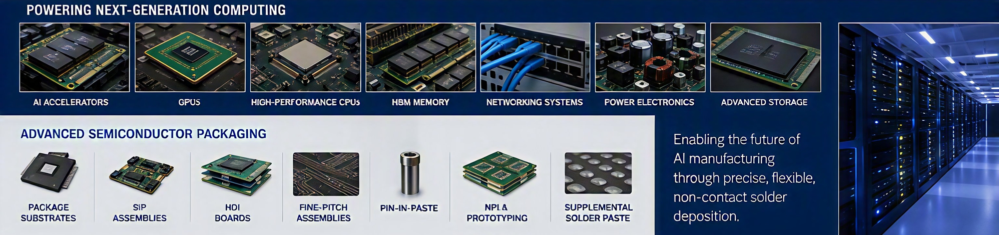
Modern AI servers and data center systems depend on increasingly sophisticated electronic architectures, including:
AI Accelerators
GPUs
High-Performance CPUs
High-Bandwidth Memory (HBM)
Networking Equipment
Power Management Modules
Advanced Storage Systems
As component densities increase and package designs become more complex, conventional stencil-based solder deposition methods can introduce limitations related to tooling, accessibility, and process flexibility.
Solder paste jetting provides manufacturers with an alternative approach that supports evolving electronics manufacturing requirements while maintaining process accuracy and repeatability.
Benefits of Non-Contact Solder Paste Jetting
Greater Manufacturing Flexibility: Jetting technology eliminates the need for dedicated stencils, allowing manufacturers to quickly adapt to design changes, prototype builds, and production volumes.
Access to Difficult-to-Reach Locations: Jetting technology eliminates the need for dedicated stencils, allowing manufacturers to quickly adapt to design changes, prototype builds, and production volumes.
Optimize Solder Volume for Boards with Mixed Component Sizes: When a PCB contains a wide range of component sizes, stencil printing can force trade-offs in solder paste volume across the board. Solder paste jetting eliminates these compromises by depositing the precise amount of solder needed at each location. This flexibility supports high-quality solder joints, improved process control, and more reliable assembly of mixed-component designs.
Reduced Tooling Requirements: By removing the need for custom stencil fabrication, manufacturers can accelerate product development cycles while reducing tooling costs.
Improved Process Efficiency: Precise volumetric control helps ensure consistent solder deposits while minimizing waste and supporting production repeatability.
Support for High-Mix Manufacturing: AI and networking hardware manufacturers often manage multiple product variants. Solder paste jetting enables faster product transitions without frequent stencil changes or process interruptions.
Supporting Advanced Semiconductor Packaging
As advanced packaging technologies become increasingly important for AI processors and high-performance computing devices, manufacturers require flexible solder deposition solutions capable of supporting evolving package architectures.
Solder paste jetting can support applications involving:
Advanced Semiconductor Packaging
Package Substrates
System-in-Package (SiP) Assemblies
High-Density Interconnect (HDI) Boards
Prototype and New Product Introduction (NPI)
Fine-Pitch Electronic Assemblies
Pin-in-Paste for Mixed-Technology Boards
Supplemental Solder Paste to expand the capabilities of an existing SMT line
Combined with precision dispensing technologies used for underfill, thermal interface materials (TIMs), and conductive adhesives, solder paste jetting helps support the manufacturing processes behind next-generation AI hardware.
Applications in Data Center Electronics Manufacturing
Solder paste jetting is commonly used in manufacturing environments that support:
AI Servers: Accurate solder deposition helps ensure reliable assembly of processor boards, accelerator modules, and server electronics designed for continuous operation.
Networking Hardware: Switches, routers, and optical networking systems require highly reliable solder connections to maintain performance within data center environments.
Power Electronics: Power delivery systems supporting modern AI infrastructure depend on robust electronic assemblies capable of handling increasing power densities.
High-Density Electronics: As component spacing decreases and board complexity increases, non-contact jetting helps maintain process precision across intricate assemblies.
Enabling the Future of AI Manufacturing
The rapid expansion of AI infrastructure continues to increase demand for advanced electronics manufacturing technologies. Solder paste jetting provides semiconductor and electronics manufacturers with a flexible, precision-driven solution for assembling the high-performance hardware that powers modern data centers.
By combining non-contact solder deposition with advanced dispensing technologies for underfill, thermal management, adhesives, and encapsulation, manufacturers can improve process control, accelerate product development, and support the next generation of AI-enabled computing systems.